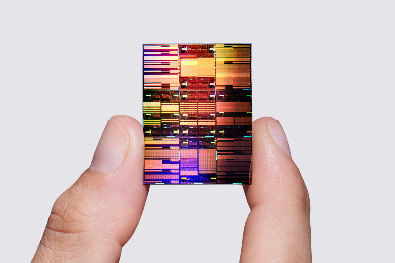
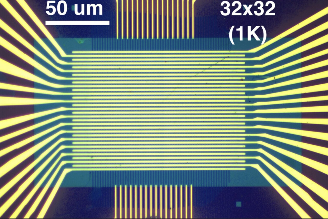
Straight out of IBM’s Zurich R&D labs are these concepts for semiconductor chips that are stacked on top of eachother and allow enough space in between for water cooling. Developed jointly with the Fraunhofer Institute in Berlin, the ‘3D’ stacking of these chips not only uses less space and allows for greater speed, but the water cooling technique could potentially take the generated heat and reuse it for other purposes. IBM says the water cooling structure is as thin as 50 microns and equal in complexity to the system of nerves and blood vessels in the human brain. Crazy stuff.[IBM via TG Daily via Engadget]