
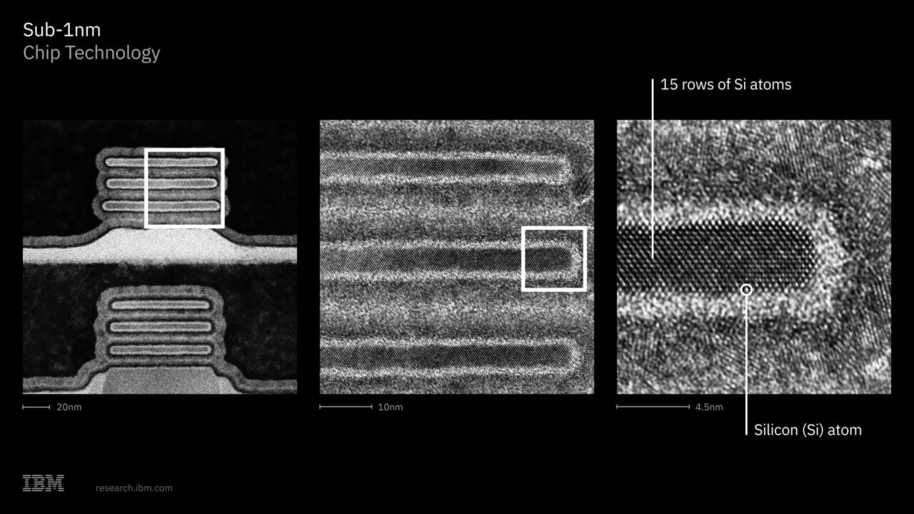
In a major breakthrough, IBM revealed the world’s first semiconductor chip technology built on a sub-1 nanometer chipmaking process. For comparison, the process uses transistor features smaller than the width of a DNA strand, which measures about 2.5 nanometers across. The chip itself is about the size of a fingernail but holds almost 100 billion transistors, and the company expects it could enter markets as early as the next five years.
In a statement released today, IBM said the new chip features nearly twice the density of its 2-nanometer chip, released in 2021. According to an accompanying technical report, the chip also demonstrated up to 70% greater energy efficiency than its predecessor. In designing the chip, researchers developed an “entirely new transistor architecture” called nanostack, which “vertically stacks and staggers transistors” to enable IBM’s 0.7-nanometer chip technology, IBM explained.
“With our new nanostack architecture, we’re not just making smaller transistors,” Jay Gambetta, director of IBM Research, said in the statement. “We’re reinventing how chips are built to deliver dramatically more power and energy efficiency.”
“I’ve spent over 20 years in the semiconductor industry at IBM, and during that time we’ve heard many times that scaling is reaching its limits,” Huiming Bu, vice president of IBM’s silicon technology research team, told Gizmodo. “What we’ve learned is that progress doesn’t stop—it just requires a new paradigm.”
Smaller and smaller
Semiconductor chips enable things like computers, home appliances, communications, and transportation devices. In 1965, Intel co-founder Gordon Moore surmised that transistor capacities evolved at a predictable and consistent rate. Specifically, all things considered, the number of transistors on a semiconductor chip would double about every two years. For a while, the so-called Moore’s Law held rather well—until, that is, things hit a literal wall.
“Moore’s Law was never meant to last forever,” according to a blog post by the Massachusetts Institute of Technology’s (MIT) Computer Science and Artificial Intelligence Lab. “Transistors can only get so small and, eventually, the more permanent laws of physics get in the way.”
That is, as companies try to cram more transistors into smaller chips, new advances in transistor technology take longer than two years, so Moore’s Law has been over since at least 2016, Charles Leiserson, a computer scientist at MIT, said in the blog. Accordingly, the issue now is to consider how improvements in chip performance fit into a longer-term picture, Willy Shih, an economist at Harvard Business School, said in an explainer.
Reaching atomic levels
In that sense, IBM’s latest chip represents an inventive approach for bypassing the limits of physical scaling. Specifically, two wafers with nanosheet-style transistors are glued together like a sandwich to vertically stack two layers of transistors, and related technical assessments suggested that the wafer stacking was flexible and scalable enough to support real computation, Bu said in a press briefing on the chip.
That said, this chip isn’t quite ready for manufacturing just yet. The company’s goal is to enter production in the next five years, but there’s still work to be done. For instance, Bu pointed out that the team was still working on pathways to prevent thermal noise or integration into existing systems in the high-performance computing community.
“From my perspective, I hope to see it be as successful as the 2-nanometer [chip] and become the industry platform,” Gambetta said during the briefing. “And as we see with AI and classical computing in general, we are only seeing more and more consumption.”
Update 06/25/2026: This story was updated after publishing to incorporate Huiming Bu’s comments to Gizmodo.